nextnano3 - Tutorial
next generation 3D nano device simulator
2D Tutorial
Electron and hole wave functions in a T-shaped strained quantum wire grown by CEO
(cleaved edge overgrowth)
Author:
Stefan Birner
If you want to obtain the input files that are used within this tutorial, please
check if you can find them in the installation directory.
If you cannot find them, please submit a
Support Ticket.
 -> 2DTshapedStrainedQuantumWireCEO.in

 -> 2DTshapedStrainedQuantumWireCEO_no_piezo.in

 -> 1DAlGaAs_InAlAs_QW.in
.
Acknowledgement: The author - Stefan Birner - would like to thank
Robert Schuster from the University of Regensburg for providing the experimental
data and some of the figures.
T-shaped strained quantum wire
This tutorial treats strained quantum wires
including a discussion of the strain calculation and the strain-induced
piezoelectric fields (Poisson equation).
Similar to the 1D confinement in a quantum well, it is possible to
confine electrons or holes in two dimensions, i.e. in a quantum wire.
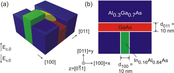
The quantum wire is formed at the T-shaped intersection of a 10 nm GaAs
type-I quantum well and a 10 nm In0.16Al0.84As
barrier (!).
The T-shaped intersection is surrounded by Al0.3Ga0.7As
which acts as a barrier to GaAs.
The In0.16Al0.84As
barrier has a larger lattice constant than Al0.3Ga0.7As
and is thus strained.
The strain affects the GaAs well and thus produces a
local decrease (increase) in the conduction (valence) band edge energy and thus
confines electrons (holes) at the T-shaped intersection.
The electrons and
holes are free to move along the z direction only, thus the wire is oriented
along the [0-11] direction.
Such a heterostructure can be manufactured by
growing the layers along two different growth directions with the CEO
(cleaved edge overgrowth) technique.
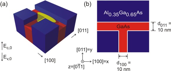
The following figure (upper part) shows the sample layout.
It is useful to
compare it to the T-shaped quantum
wire tutorial (lower part of the figure) which consists of two GaAs quantum
wells rather than one GaAs well and one In0.16Al0.84As
barrier in order to understand the fundamental difference between these two
layouts.
|
This tutorial (T-shaped strained quantum wire):
T-shaped quantum wire tutorial:
 |
|
(a)
The figure at the top schematically shows the conduction band profile
without considering strain effects (!) of
the T-shaped wire that was grown by the CEO technique. If one inverts the
energy arrow then the left picture corresponds to the valence band edge.
The wave function is indicated at the T-shaped intersection in yellow.
In the figure at the bottom,
the wave function can extend into a larger volume (as compared to the quantum
well) and thus reduce its energy. So quantum mechanics tells us that the
ground state can be found at this intersection and electrons are only
allowed to move one-dimensionally along the z direction. For the figure at
the top, this is not true. The confinement only occurs if one
takes into account the strain which decreases (increases) the conduction
(valence) band edge energy in GaAs at the T-shaped intersection.
(b)
The figures on the right show a 60 nm x 60 nm extract of the schematic layout including the
dimensions, the material composition and the orientation of the wire with
respect to the crystal coordinate system.
|
It is sufficient to describe this heterostructure within a 2D simulation as
it is translationally invariant along the z direction.
The simulation coordinate system is oriented in the following way:
 $domain-coordinates


  domain-type        =
1  1  0  !
  hkl-x-direction-zb = 1  0  0
! [100] direction in the crystal coordinate
system
  hkl-y-direction-zb = 0  1  1
! [011] direction in the crystal coordinate
system
! hkl-z-direction-zb = 0 -1 1 ! [0-11] direction in the crystal
coordinate system
hkl-z-direction does not have to be specified. It
is calculated internally in the code.
The simulations are performed at 4 Kelvin:
 $global-parameters

  lattice-temperature = 4.0d0   !
[K]
The lattice constants are temperature dependent.
$numeric-control
  lattice-constants-temp-coeff-on = yes
! temperature dependent lattice constants
Our sample is simulated on a domain which has an extension of 310 nm along
the x direction and 410 nm along the y direction.
Calculation of the strain tensor
First, we have to calculate the strain tensor by minimizing the elastic
energy within continuum elasticity theory.
Along the translationally invariant z
direction the lattice commensurability constraint forced the In0.16Al0.84As
layer to adopt the lattice constant of Al0.3Ga0.7As.
 $simulation-flow-control

  ...

  strain-calculation = strain-minimization
 $strain-minimization-model
!
for "strain-calculation = strain-minimization"
substrate-cluster-number = 4
! Here one specifies the relevant cluster that acts as the (unstrained)
substrate. (here: Al0.3Ga0.7As)
  boundary-condition-x     =
Neumann  !
  boundary-condition-y     =
Neumann  !
  boundary-condition-z     =
periodic !
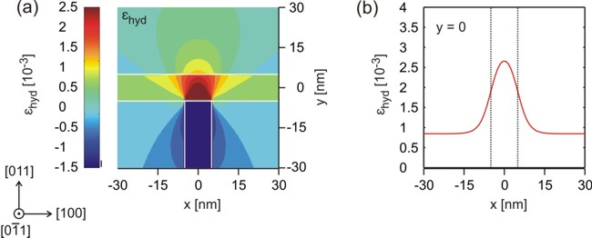
The hydrostatic strain (trace of the strain tensor, i.e. ehydro =
exx + eyy + ezz), i.e. relative change in
volume) has its maximum at the intersection,
where it leads to a reduced band
gap which is the requirement for confining the charge carriers.
Thus, the
quantum wire is formed in the GaAs quantum well due to the tensile strain field
induced by the In0.16Al0.84As layer.
|
 |
|
(a) The figure shows the hydrostatic strain.
It can be cleary seen that the maximum volume deformation (red:
tensile strain) occurs at the T-shaped intersection, thus
reducing the band gap at this position and providing a confinement for both
electrons and holes.
(b) This is a cut through figure (a) at position y=0.
The data shwon in this plot can be found in the file:
strain/e_hydro2D_slice_middle_range_along_x.dat
Note: The scale on the left figure is wrong. The
dark blue area should have the value -15
rather than -1.5.
The reason is due to the color map. All values below -1.5 have the same
color (dark blue). |
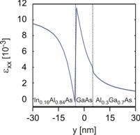
Note: In a one-dimensional example, the strain tensor components of an In0.16Al0.84As
layer that is strained pseudomorphically with respect to an Al0.3Ga0.7As
substrate are the following:
exx = 0.01096 = 11 * 10-3
eyy = ezz = -0.01245 = -12 * 10-3
exy = exz = eyz = 0
ehydro = Tr(eij) = -0.01393 = -14 * 10-3
The growth direction is along the x direction, i.e. along [100]. The
relevant input file is 1DAlGaAs_InAlAs_QW.in.
These strain tensor components can be found in the file:
strain/strain_cr1D.dat
The temperature is assumed to be 4 Kelvin and the lattice constants are
assumed to be temperature dependent (i.e. we use the 4 K lattice constants).
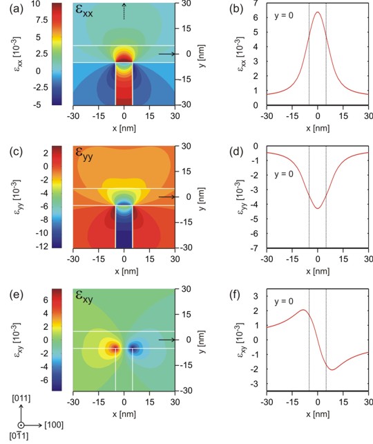
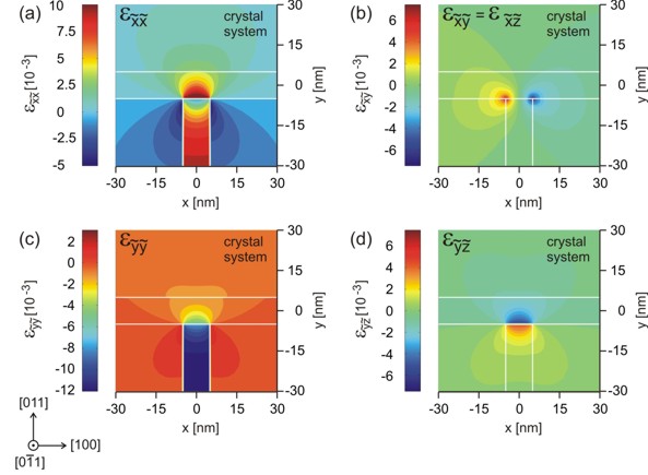
The individual strain tensor components (exx, eyy, exy)
with respect to the simulation coordinate system look like this:
|
 |
 |
|
(a), (c), (e) The color maps on the left show the
strain tensor components exx, eyy and exy.
(b), (d), (f) show a cut through the color maps for y=0.
The picture at the upper right corner shows the cut for x=0 of the strain
tensor component exx. |
In our 2D simulation, our sample layout is homogeneous along the z direction,
i.e. the lattice constant of In0.16Al0.84As is forced to
have the same lattice constant as Al0.3Ga0.7As along the z
direction. Then the strain tensor component must be ezz =
-0.01245, in agreement with our 1D example, i.e. In0.16Al0.84As
which has a larger lattice constant than Al0.3Ga0.7As is
strained compressively along the z direction. Similar to the 1D case, it is also
expected that the eyy component inside the In0.16Al0.84As
barrier has a similar value to ezz, which is clearly
the case. The dark blue area in Fig. (c)
thus has a value around -12 * 10-3. However, this value
deviates from the ideal 1D value at the T-shaped intersection as expected. The
same applies to the value of exx which is similar to the
1D value inside the In0.16Al0.84As barrier: exx = 11 * 10-3
The strain tensor components exz and eyz
with respect to the simulation coordinate system re equal to zero as in our 1D example.
The important difference with respect to the 1D case is the existence of a
non-vanishing strain tensor component exy which brakes
the symmetry of the sample layout.
Usually, the exy component is attributed to be responsible for piezoelectricity.
However, note that in these comments, all strain tensor components refer to the
simulation
coordinate system (and not to the crystal coordinate system). So we have to
plot the off-diagonal strain tensor components that are expressed with respect
the crystal coordinate system orientation and then check if the off-diagonal
components are non-zero which clearly is the case.
|
 |
|
The color maps show the strain tensor
components exxcr, eyycr, exycr=exzcr
and eyzcr with respect to the crystal coordinate
system.
The rotation with respect to the simulation system is a rotation of 45
degrees around the x axis, i.e. the [100] axis. |
Clearly, Fig. (a) shows that exxcr = exx
because the x coordinate axes coincide. Symmetry arguments show that the
following holds:
eyycr = 1/2 ( eyy + ezz )
exycr = exzcr = 1/SQRT(2) exy
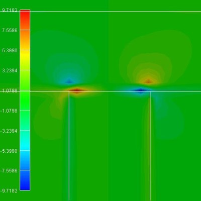
Calculation of the piezoelectric charge density
The off-diagonal strain tensor components exycr, exzcr
and eyzcr are responsible for the piezoelectric
polarization where e14 is the piezoelectric constant in units
of [C/m²]:
( 2 eyzcr )
Ppiezo = e14 ( 2 exzcr
)
( 2 exycr )
Once having determined the piezoelectric polarization Ppiezo
one is able to compute the piezoelectric charge density: ρpiezo(x)
= - div Ppiezo(x).
The strain-induced piezoelectric fields are then obtained by solving Poisson's
equation.
|
 |
|
The piezoelectric charge density in units of 1
* 1018 e/cm³. |
Calculation of the conduction and valence band edges
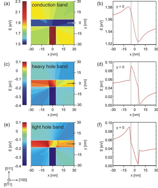
The new conduction and valence band edges were determined by taking into
account the shifts and splittings due to the relevant deformation potentials as
well as the changes due to the piezoelectric fields.
|
 |
|
(a), (c), (e) Color maps of the conduction,
heavy hole and light hole band edge energies.
(b), (d), (f) A cut through the conduction, heavy hole and light hole band
edge energies at y=0.
Very interestingly, one can see that the electron feels a conduction band
minimum which is located left with respect to the T-shaped intersection. The
valence band maximum for the heavy hole is not at the same position as the
valence band maximum for the light hole. |
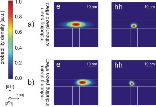
Electron and heavy hole wave functions
The size of the quantum cluster is 110 nm x 110 nm.
The following figure shows the square of the electron (e) and heavy hole (hh)
wave functions (i.e. psi²). They were calculated within the effective-mass
approximation (single-band). For the holes we derived the effective mass tensor
from the Luttinger parameters to include anisotropy. For the upper part of the
figure the piezo effect was not included. As one can clearly see in the lower
part of the figure, the piezo effect destroys the symmetry of the sample layout.
The piezoelectric field results from the exy strain tensor component
which is also not symmetric with respect to the T-shaped geometry.
|
 |
|
a) Contour diagram of the square of the
electron (e) and heavy hole (hh) wave functions (i.e. psi²) for the case
where strain is included in the simulations but piezoelectricity is not.
b) Same as in a) but this time including the
piezo effect.
Note: Here, the wave functions are normalized so that the
maximum of each equals one.
The size of the shown squares is 60 nm x 60 nm whereas the size of the
quantum cluster was chosen to be 110 nm x 110 nm. |
More details can be found in the following PhD thesis:
Hochortsaufgelöste optische Spektroskopie an
niedrigdimensionalen Halbleiterstrukturen
Robert Schuster
University of Regensburg (2005)
In this thesis the "confinement energy" is defined as the difference between the transition
energies of the quantum wire and the quantum well.
They can be calculated with the nextnano software as a function of alloy
content or well widths.
In this thesis, excitonic effects were not included.
|