|
| |
nextnano3 - Tutorial
next generation 3D nano device simulator
1D Tutorial
GaN/AlN wurtzite structure: Strain, piezo and pyroelectric charges in
wurtzite
Author:
Stefan Birner
-> 1Dwurtzite_nn3_noStrain_noPiezo_noPyro_noPoisson.in
-
input file for the nextnano3 software
-> 1Dwurtzite_nn3.in
/ *_nnp.in  -
-> 1Dwurtzite_nn3_Nface.in
/ *_nnp.in  -
These input files are included in the latest version.
GaN/AlN structure
- This input file simulates a GaN/AlN/GaN wurtzite structure:
1Dwurtzite.in
The structure is grown pseudomorphically on GaN, i.e. the AlN is
tensilely strained, the GaN is unstrained. The growth direction [0001]
is along z, the interfaces are in the (x,y) plane. As we have [0001] growth
direction, we have Ga-polar GaN (i.e. Ga-face polarity).
- No strain.
$numeric-control

 simulation-dimension
  = 1

 zero-potential
  = yes

   varshni-parameters-on           = no  !
Band gaps independent of temperature.
Absolute values from database are taken.
lattice-constants-temp-coeff-on = no !
Lattice constants independent of temperature.
Absolute values from database are taken.
 piezo-constants-zero
  = yes !
Piezoelectric constants are set to
zero.
 pyro-constants-zero
  = yes !
Pyroelectric constants are set to
zero.
$end_numeric-control
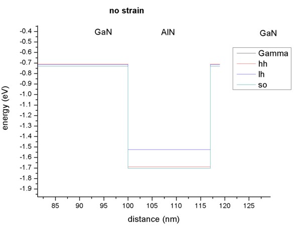
- The pictures shows the conduction and valence band edges of the
heterostructure when no strain is applied (
strain-calculation =
  no-strain
). AlN is the barrier
for both electrons and holes.
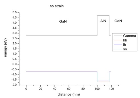
Now we zoom into the valence band structure. In AlN the light hole lies above
the heavy hole, in GaN the situation is the opposite. Note that heavy and
light hole are not degenerate (as would be the case in zinc blende).
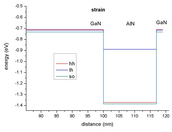
- Pseudomorphic strain.
strain-calculation =
  homogeneous-strain

  pseudomorphic-on   = GaN !
lattice constant a=0.3189 nm (lattice constant c does not matter
for this growth direction)
The biaxial strain is tensile: eps|| = (asubstrate -
a)
/ a = 0.0247429
The uniaxial strain is compressive: eps_|_= - 2 c13/c33
eps|| = - 0.0143283
The hydrostatic strain is positive which corresponds to an increase in volume
for AlN: epshy = Tr(epsij) = (2 eps|| + eps_|_)
= 0.0351575
The strain leads to a shift in the conduction and valence band edges.
Conduction band at Gamma:
In wurtzite the crystal anisotropy leads to two distinct conduction band
deformation potentials for the Gamma point, one is parallel and the other one
is perpendicular to the c axis.
absolute-deformation-potentials-cbs = ac,a axis
ac,a axis ac,c axis
 absolute-deformation-potentials-cbs =
   -3.9d0  -3.9d0 -20.5d0 ! [eV]
Thus the conduction band edge energy including the hydrostatic
energy shift is given by:
-20.5
* (-0.0143283) ) + 2 (-3.9) *
0.0247429 = 4.712 + 0.10073553 = 4.81274 eV
So in this particular example, the barrier for electrons is increased.
uniax-cb-deformation-potentials-cbs = 0d0 0d0 0d0
Data for uniaxial deformation potentials of other minima than
Gamma are not available yet. At the Gamma point, the uniaxial deformation
potential is zero.
Valence bands:
From a full treatment of the effect of strain on the six-band Hamiltonian
six valence band deformation potentials arise.
 uniax-vb-deformation-potentials     =
     d1    d2
  d3    d4    d5    d6  !
  [eV]

 uniax-vb-deformation-potentials     =
  -17.1   7.9   8.8  -3.9
  -3.4  -3.4  ! [eV]
In contrast to zinc blende, an absolute deformation potential for the
valence band is not needed.
 absolute-deformation-potential-vb   =
  0d0 !
(Not needed, should be removed from
wurtzite database in the future.)
The shifts of the valence bands are obtained by diagonalizing the Bir-Pikus
strain Hamiltonian which is given in
Basics 2 (strain
effects). This is a general approach as it gives the correct shifts for
arbitrary orientations (However, it is only for valence bands).
In our example, the tensile strain in AlN shifts all holes upwards,
- the heavy hole by 0.31687 eV,
- the light hole by 0.63565 eV and
- the crystal field split-off hole by 0.31717 eV,
thus reducing the barrier for the holes.
- Pyroelectric polarization (spontaneous polarization)
$numeric-control

 pyro-constants-zero = no
The wurtzite materials GaN, AlN and InN are pyroelectric materials and
thus show a spontaneous polarization.
Thy pyroelectric field Ppy is along the hexagonal z
direction (along c axis) and it is always negative. Ppy is
directed from anion to cation. The positive z direction (i.e. [0001]) is from
cation to anion.
GaN: Ppy = - 0.034 C/m²
AlN: Ppy = - 0.090 C/m²
At the interfaces we have a discontinuity of Ppy(z).
The pyroelectric polarizations at the interfaces are determined as follows:
1st interface at 100 nm (GaN/AlN): Ppy(left point)
- Ppy(right point) = - 0.034 + 0.090 = 0.056 C/m²
2nd interface at 117 nm (AlN/GaN): Ppy(left point) - Ppy(right
point) = - 0.090 + 0.034 = - 0.056 C/m²
The interface charges can be found in the output file
interface_densitiesD.txt ($output-densities).
The interface charge of -0.056 C/m² corresponds to 34.952*1012
electrons /cm².
Once having determined the pyroelectric polarization Ppy one
is able to compute the pyroelectric charge density: rhopy(x) =
- div Ppy(x).
If the hexagonal axis is oriented along the z axis as in our example, this
equation reduces to: rhopy(z) = - d/dz Ppy(z)
The pyroelectric charge density per cm³ is given in density1Dpyro.dat.
In pyro_polarization.dat the pyroelectric constant as given in
the database or input file is plotted for each grid point.
- Piezoelectric polarization
$numeric-control

 piezo-constants-zero = no
If AlN is strained, piezoelectric fields arise.
In GaN the piezoelectric polarization is zero as there is no strain.
AlN: e33 = 1.79, e31 = - 0.50 (e15 is not
relevant for [0001] growth direction)
In AlN the piezoelectric polarization is:
Ppz = e33eps_|_ + e31 (eps||
+ eps||) = 1.79 * (- 0.0143283) - 0.50 * 2 * 0.0247429 =
-
0.050390 C/m²
Ppz is directed in this example parallel to Ppy
as the piezoelectric polarization is negative for tensilely strained AlN grown
on GaN.
GaN: Ppz = 0 C/m² (no strain)
AlN: Ppz = - 0.050390 C/m²
At the interfaces we have a discontinuity of Ppz(z).
The piezoelectric polarizations at the interfaces are determined as follows:
1st interface at 100 nm (GaN/AlN): Ppz(left point)
- Ppz(right point) = 0 + 0.050390 = 0.050390 C/m²
2nd interface at 117 nm (AlN/GaN): Ppz(left point) - Ppz(right
point) = - 0.050390 - 0 = - 0.050390 C/m²
The interface charges can be found in the output file
interface_densitiesD.txt ($output-densities).
The interface charge of -0.050390 C/m² corresponds to 31.451*1012
electrons /cm².
Once having determined the piezoelectric polarization Ppz
one is able to compute the piezoelectric charge density: rhopz(x)
= - div Ppz(x).
The piezoelectric charge density per cm³ is given in density1Dpiezo.dat.
In our 1D example, this equation reduces to: rhopz(z) = - d/dz Ppz(z)
In piezo_polarization.dat the piezoelectric constants (e33,
e31, e15) as given in the database or input file are
plotted for each grid point.
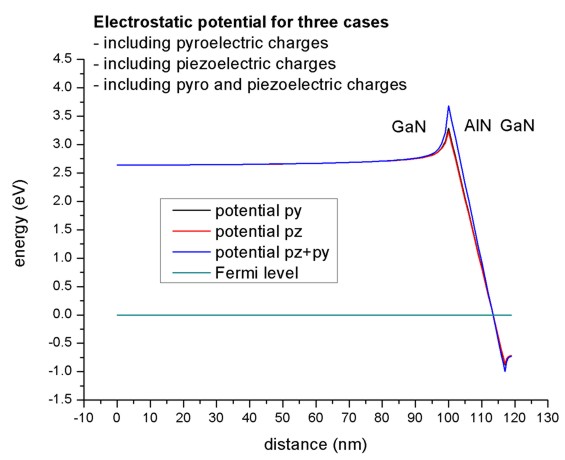
- Electrostatic potential including piezo and pyroelectric charges.
The electrostatic potential is the solution of the nonlinear Poisson
equation.
- div (ε(r) grad phi(r)) = rho(r,phi)
The charge density rho contains the (static) piezo and pyroelectric
charge densities as well as the electron and hole charge
densities and ionized donors and acceptors. The latter depend on
the electrostatic potential phi but the piezo and pyroelectric charge
densities don't.
(zero-potential = no)
Here we plot the electrostatic potential in units of eV for three different
cases:
- including pyroelectric charges
(piezo-constants-zero = no ,
pyro-constants-zero = yes)
- including piezoelectric charges
(piezo-constants-zero = yes,
pyro-constants-zero = no)
- including pyro and piezoelectric charges
(piezo-constants-zero = no ,
pyro-constants-zero = no)
In our example the piezo and pyroelectric contributions are of the same size.
The Fermi level is set to zero.
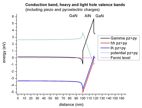
- The electrostatic potential in units of eV has to be substracted from the
conduction and valence band edges. The resulting band structure is plotted in
this figure (The piezo and pyroelectric charges were considered in this
calculation).
Note that the conduction band is pulled below the Fermi level (around 98 nm)
and the valence band above the Fermi level (around 118 nm).
N-face polarity
This input file simulates a GaN/AlN/GaN wurtzite structure (N-face polarity):
1Dwurtzite_Nface.in
The structure is the same as above. The only difference is the polarity:
N-face instead of Ga-face.
The above examples correspond to Ga-face polarity. In order to
investigate N-face polarity, we have to switch from [0001] growth
direction to [000-1] growth direction (z -> -z). In order to keep a
right-handed coordinate axes system we also invert the x direction (x ->
-x). The third direction (here: the y direction) is calculated
automatically (internally).
 $domain-coordinates

  domain-type
= 0 0 1

  z-coordinates          =
0.0d0 119d0

  growth-coordinate-axis = 0 0 1
!
along z direction
  pseudomorphic-on       =
GaN


  !********************************

  ! This is along [0001] direction: Ga-face polarity


  ! hkil-x-direction =  1 0 -1 0
! [ 1 0 -1 0]
!!hkil-y-direction = -1 2 -1 0
! Miller-Bravais indices of y coordinate axis [-1 2 -1 0]
! hkil-z-direction = 0 0 0 1
! Miller-Bravais indices of z coordinate axis [ 0 0 0 -1]
! Equivalent Bravais indices
! hkl-x-direction-zb = 1 0 0
! Miller indices of x coordinate axis
[1 0 0]

  ! hkl-y-direction-zb = 0 1 0
!
Miller indices of y coordinate axis [0 1 0]
! hkl-z-direction-zb = 0 0 1
! Miller indices of z coordinate axis
[0 0 1]

  !********************************


  !********************************

  ! This is along [000-1] direction: N-face polarity


    hkil-x-direction = -1 0  1  0
! => -x !
Miller-Bravais indices of x
coordinate axis [-1 0
1 0]
! hkil-y-direction = -1 2 -1 0
! Miller-Bravais indices of y coordinate axis [-1 2 -1 0]
hkil-z-direction = 0 0 0 -1
! => -z ! Miller-Bravais indices of z
coordinate axis [ 0 0 0 -1]
! Equivalent Bravais indices
! hkl-x-direction-zb = -1 0 0
! Miller indices of x coordinate axis
[1 0 0]

  ! hkl-y-direction-zb =  0  1  0
!
Miller indices of y coordinate axis [0 1 0]
! hkl-z-direction-zb = 0 0 -1
! Miller indices of z coordinate axis [0 0 1]
!********************************
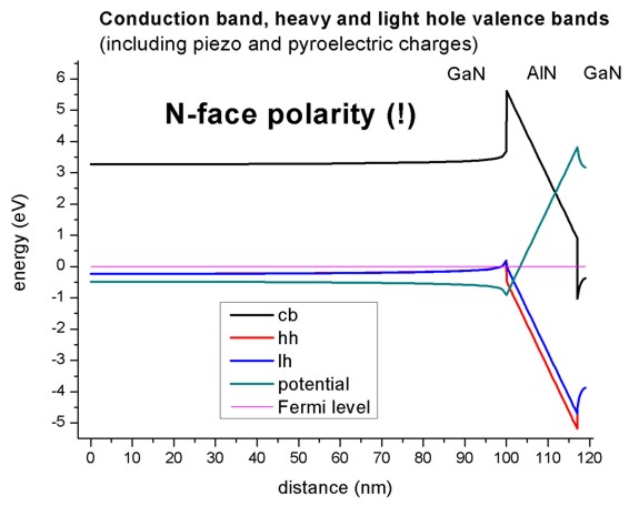
The figure shows the Fermi level (at 0 eV), the electrostatic potential and the
conduction and valence band edges (heavy and light hole) of the N-face
heterostructure.
(The piezo and pyroelectric charges were considered in this
calculation).
Note the difference in comparison to the figure above for the Ga-face case.
The location of the 2DEGs and 2DHGs (two-dimension hole gases) is reversed.
An alternative way of switching from Ga-face to N-face would have been to
change the sign of the pyroelectric constants.
The boundary conditions for the Poisson equation in this simulation were
Neumann boundary conditions, i.e. the derivative of the electrostatic potential
is zero at the boundaries (flat band boundary conditions).
No doping was present in this simulation.
Note: The figures shown in this tutorial have been generated a long time
ago. The actual results may differ from these figures because the input files
now contain a modified grid space resolution, and modified layer widths, as well
as a different total structure size.
|