nextnano3 - Tutorial
next generation 3D nano device simulator
2D Tutorial
Ultrathin-body Double Gate FET - DG MOSFET (Double Gate Metal Oxide Semiconductor Field Effect
Transistor) (5 nm)
Author:
Stefan Birner
If you want to obtain the input files that are used within this tutorial, please
check if you can find them in the installation directory.
If you cannot find them, please submit a
Support Ticket.
 -> 2DDoubleGateMOSFET_cl.in

 -> 2DDoubleGateMOSFET_qm.in
Ultrathin-body Double Gate FET - DG MOSFET (Double Gate Metal Oxide Semiconductor Field Effect
Transistor) (5 nm)
Some of these figures are included in this publication:
Modeling of semiconductor nanostructures with nextnano³
S. Birner, S. Hackenbuchner, M. Sabathil, G. Zandler, J.A. Majewski, T.
Andlauer, T. Zibold, R. Morschl, A. Trellakis, P. Vogl
Acta Physica Polonica A 110 (2), 111 (2006)
Structure
The main idea of a Double Gate MOSFET is to control the Si channel very
efficiently by choosing the Si channel width to be very small and by
applying a gate contact to both sides of the channel. This concept helps to
suppress short channel effects and leads to higher currents as compared with
a MOSFET having only one gate.
The structure consists of an intrinsic Si channel having the length 25 nm and
the width 5 nm.
(The width of 25 nm corresponds to the 65 nm technology node.)
This channel is connected to heavily n-type doped source and drain regions of
length 10 nm each (constant doping profile with a concentration of 1 x 10²⁰
cm-3, fully ionized).
The gates have a length of 25 nm and are separated from the Si channel by a 1.5
nm thick oxide layer.
(SiO2, static-dielectric-constants =
3.9d0)
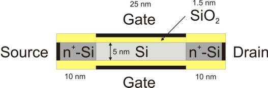
The Double Gate MOSFET contains the following regions
|
cluster |
region |
|
| 1 |
1 |
Source contact |
| 2 |
2 |
n-type doped source region (Si) |
| 3 |
3 |
Si channel (undoped) |
| 4 |
4 |
n-type doped drain region (Si) |
| 5 |
5 |
Drain contact |
| 6 |
6 |
SiO2 |
| 7 |
7 |
Top gate |
| 7 |
8 |
Bottom gate |
Both the regions 7 (top gate) and 8 (bottom gate) form the cluster no. 7.
Along the channel direction (x direction), the grid lines are separated by 1 nm
(48 grid points),
along the y direction, the grid lines have a 0.5 nm separation (21 grid lines).
The total number of grid points is 48 x 21 = 1008.
Contacts
We apply a voltage of VD = 0.5 V to the drain contact.
The gate voltage is varied from -0.3 V to 1.0 V in steps of 0.1 V (=>
$voltage-sweep).
At the gate a Schottky barrier of 3.075 V is assumed to mimick the gate
electrode work function which has been assumed to be 4.1 eV.
 $poisson-boundary-conditions


  poisson-cluster-number  = 1
!
Source
  region-cluster-number   = 1

  applied-voltage         =
0.0d0      ! 0.0 [V]

  boundary-condition-type = ohmic

  contact-control         =
voltage


  poisson-cluster-number  = 2
!
  region-cluster-number   = 5

  applied-voltage         =
0.5d0      ! 0.5 [V]

  boundary-condition-type = ohmic

  contact-control         =
voltage


  poisson-cluster-number  = 3
!
  region-cluster-number   = 7

  applied-voltage         =
-0.3d0     ! -0.3 [V] ... 1.0
[V]

  boundary-condition-type = Schottky

  schottky-barrier        =
3.075d0    ! phi_B

  contact-control         =
voltage


 $end_poisson-boundary-conditions
 $voltage-sweep

  sweep-number
= 1

  sweep-active
= yes

  poisson-cluster-number  = 3
! Gate: poisson-cluster-number = 3
step-size
= 0.1d0 ! voltage
steps of 0.1 [V]
number-of-steps =
13
data-out-every-nth-step = 1
Mobility
The mobility is assumed to depend on temperature (T = 300 K) and on the
doping concentration but is independent of the electric field.
$simple-drift-models

   mobility-model = mobility-model-simba-0
!  =>
$mobility-model-simba
Thus we have two different electron mobilities:
- n-type doped Si region: 64.47 cm2/Vs
µ = 55.2 cm2/Vs + 1374.0 cm2/Vs
/ [ 1 + ( 1.0*1020 / 1.072*1017)0.73 ] =
64.470195 cm2/Vs
- intrinsic Si region: 1429.2 cm2/Vs
µ = 55.2 cm2/Vs + 1374.0 cm2/Vs
= 1429.2 cm2/Vs
Results
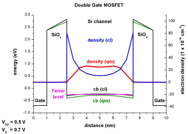
Electron density and conduction band profile
The following figure shows a slice through the middle of the device
(x=constant), i.e. through the gate contacts.
The source drain voltage is VSD = 0.5 V, and the gate voltage is VG
= 0.7 eV.
Two results are shown:
a) classical calculation
self-consistent solution of the two-dimensional
Poisson and current equations
The current equation is solved within a drift-diffusion model
based on the classical density.
b) quantum mechanical calculation
self-consistent solution of the two-dimensional
Poisson, Schrödinger and current equations
The current equation is solved within a drift-diffusion model
based on the quantum mechanical density.
The Schrödinger equation has to be solved each time three
times because of the different orientations of the
ellipsoidal electron effective mass tensors (mlongitudinal = 0.916 m0
and mtransversal
= 0.190 m0).
The Fermi level is almost flat, i.e.
constant (-0.249 eV) and very similar in both simulations a) and b).
The conduction band edge in the Si
channel is lower in the case of the quantum mechanical simulation b).
The main difference is attributed to the electron density:
a) The classical density has its
maximum at the Si/SiO2 interface
because EF,n - EC
has its maximum there, i.e. the conduction
band edge is farthest below the Fermi level.
b) The quantum mechanical density is
practically zero at the Si/SiO2 interface because
due to the SiO2 barrier, the wave functions tends
to zero at the Si/SiO2 interface.
One can clearly see that the electron density has the highest values in
the middle of the channel
and not at
the Si/SiO2 interfaces.
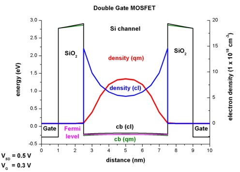
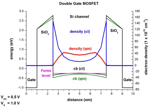
The same figures as above but this time
- left figure: at a gate voltage of 0.3 V (closed channel) and
- right figure: at a gate voltage of 1.0 V (open channel).
The quantum mechanical density has different shapes at different voltages (one
maximum in the middle vs. two maxima off-the-center).
(Note: The axes are scaled differently.)
Electron wave functions
There are three Schrödinger equations that have to be solved each time having
the following mass tensors that enter into the Hamiltonian H(x,y):
- mxx = mlongitudinal = 0.916 m0
and myy = mzz = mtransversal
= 0.190 m0
- myy = mlongitudinal = 0.916 m0
and mxx = mzz = mtransversal
= 0.190 m0
- mzz = mlongitudinal = 0.916 m0
and mxx = myy = mtransversal
= 0.190 m0
Note that mzz(x,y) does not enter the Hamiltonian but mzz(x,y)
is used to calculate the quantum mechanical density (m|| dispersion).
The quantum mechanical density for such a two-dimensional simulation is
proportional to the square root of mzz(x,y).
The quantum mechanical density is obtained for each grid point by
- summation over all eigenstates Ei
- evaluation of the square of the wave function psi(x,y)2
- weighting psi(x,y)2 with the Fermi-Dirac integral F-1/2[ (EF
- Ei) / kBT ] (which includes the Gamma prefactor of the
Fermi-Dirac integral)
- multiplication by a factor (spin and valley degeneracy / (surface of
grid point), square root of (mzz kBT / (2 pi hbar2))
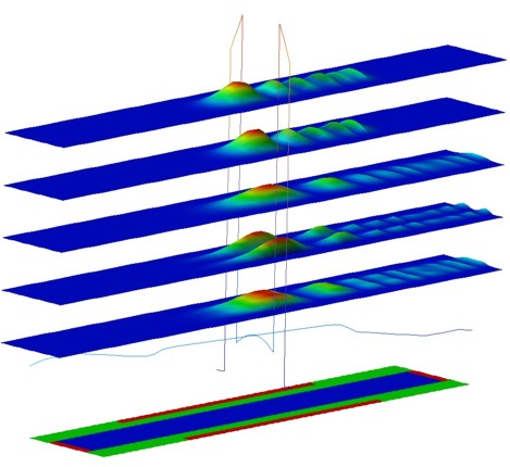
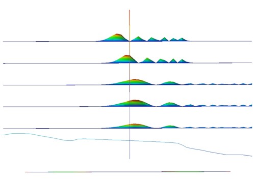
Most of the wave functions are located in the source and drain region (not
shown in the figure below).
This figure shows some of the lowest wave functions (psi2) that
contribute to the quantum mechancial density in the region where the 1D slice
was taken (i.e. in the middle of the device (VG = 0.7 V, VSD
= 0.5 V).
The Fermi energy along the 1D slice through the middle of the device lies at
-0.249 eV.
The states are labelled from top to bottom:
(Note: They are sorted by energies but their distance is not equivalent to their
energy spacing.)
deg1:    35th state
-0.215 eV (psi2 is zero at the 1D slice which can be seen in
the right figure)
deg1: 32nd state -0.224 eV
deg3: 13th state -0.226 eV
  deg2:    32nd
  state    -0.250 eV
  deg2:    25th
  state    -0.277 eV
deg1: These are the states originating from the valleys having
the light, transversal mass perpendicular to the channel
(i.e. these
states have higher energies).
deg3:
deg2: These
are the states originating from the valleys having the heavy, longitudinal
mass perpendicular to the channel
as is the
case in standard MOSFETs (i.e. these are the states that are occupied because
the energies are the lowest).
Output
- The band structure (conduction and valence bands) and the electrostatic
potential will be saved into the directory band_structure/.
densities/.
current/.
raw_data/.
I-V characteristics (current-voltage characteristics)
- The current-voltage (I-V) characteristic can be found in the following
file:
current/IV_characteristics2D.dat
The drain voltage has been kept constant at 0.5 V, the gate voltage varied from
-0.3 V to 1.0 V.
Due to the influence of quantum mechanics a shift of the threshold voltage
Vth to a slightly higher voltage can be seen.
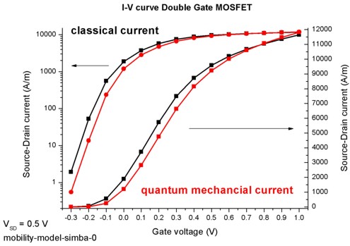
Note that the absolute magnitude of the current is
determined mostly by the mobility model.
By using a more realistic mobility model that takes into account the
dependency of the parallel and perpendicular electric fields, a smaller
current would be obtained.
a) To calculate the I-V characteristics for the classical simulation (13 voltage steps from
-0.3 V to 1.0 V), it took about 30 minutes.
(Linux executable for 64-bit Opteron)
b) To calculate the I-V characteristics for the quantum mechanical simulation (13 voltage steps from
-0.3 V to 1.0 V), it took about minutes.
(Windows executable for 64-bit Opteron)
|