|
| |
nextnano3 - Tutorial
next generation 3D nano device simulator
1D Tutorial
Electron concentration in doped semiconductors (Si, Ge, GaAs) - Compensated
semiconductors
Author:
Stefan Birner
If you want to obtain the input files that are used within this tutorial, please
check if you can find them in the installation directory.
If you cannot find them, please submit a
Support Ticket.
1) -> 1Dn_doped_bulk_Si.in

2) -> 1Dn_doped_bulk_GaAs.in

3) -> 1Dn_doped_bulk_Ge_a.in

3) -> 1Dn_doped_bulk_Ge_b.in

4) -> 1Dn_doped_bulk_Ge_a_compensated.in

5) -> 1Dn_doped_bulk_Ge_a_compensated_two_donors.in
1) Effective density of states Nc(T) of the conduction band in Si
and GaAs
The effective density of states Nc(T) of a conduction band is
defined as
Nc(T) = 2 (2 pi me
kBT / h² )3/2
2: spin degeneracy factor
For an effective mass of me = 1 at a temperature of 300 K, the value
of Nc = 25.09*1018 cm-3.
The same equation holds for the effective density of states Nv(T) of
a valence band where the valence band mass mh has to be used.
Note that some of the conduction bands are degenerate (valley degeneracy), e.g.
- the X conduction band minimum in a zinc
blende semiconductor
is three-fold degenerate, so N'c(T) =
3 Nc(T). (Note: Each valley counts only
1/2 because they are at the boundary of the Brillouin zone.)
- the Delta conduction band minimum in silicon is six-fold degenerate, so N'c(T) =
6 Nc(T). (Note: Each valley counts
because they are not at the boundary of the Brillouin zone.)
- the L conduction band minimum in germanium is four-fold
degenerate, so N'c(T) = 4 Nc(T).
(Note: Each valley counts only 1/2 because they are at the boundary of the
Brillouin zone.)
1a) Si
In silicon, the
electron mass at the X valley is an ellipsoid with a longitudinal and two
transverse masses:
  conduction-band-masses = 0.156d0
    0.156d0  0.156d0 ! GAMMA: m,m,m


    1.420d0  0.130d0  0.130d0 ! L: ml,mt,mt


    0.916d0  0.190d0  0.190d0 ! X: ml,mt,mt
The density of states mass is calculated as follows:
The value of
kBT at different temperatures reads:
- T = 10 K:
kBT = 0.86173 meV
- T = 100 K:
kBT = 8.6173 meV
- T = 300 K:
kBT = 25.852 meV
Thus for Si we obtain the following values for the effective density of
states Nc(T) at the sixfold X (i.e.
Delta) conduction band minimum:
- T = 10K:
Nc = 6 * 2
(2 pi me
kBT / h² )3/2 = 2 (0.321 *
0.8617*10-3 * 2.0886*1014)3/2
= 0.166626 * 1018 cm-3
- T = 100K:
Nc = 6 * 2
(2 pi me
kBT / h² )3/2 = 2 (0.321 *
8.617*10-3 * 2.0886*1014)3/2
= 5.26919 * 1018 cm-3
- T = 300K:
Nc = 6 * 2
(2 pi me
kBT / h² )3/2 = 2 (0.321 *
25.85*10-3 * 2.0886*1014)3/2
= 27.3795 * 1018 cm-3
The output for Nc is contained in the following file:
Nc_cb1D.dat
The units are 1 * 1018 cm-3.
The first column refers to Nc of the conduction band at the Gamma
point, the second at the L point, and the third at the X (or Delta) point.
For the valence bands, the effective density of states of the heavy (hh), light
(lh) and split-off (so) hole bands are contained in the file:
Nv_vb1D.dat: Nv(hh), Nv(lh), Nv(so)
To vary the temperature, the following specifier has to be varied:
 $global-parameters

 !lattice-temperature =  10.0d0  !
10 Kelvin
!lattice-temperature = 100.0d0 !
lattice-temperature = 300.0d0 !
$end_global-parameters
1b) GaAs
For GaAs where the electron mass at the Gamma point is me = 0.067
m0 we obtain:
- T = 10K:
Nc = 2 (2 pi me
kBT / h² )3/2 = 2 (0.067 *
0.8617*10-3 * 2.0886*1014)3/2
= 0.00264852 * 1018 cm-3
- T = 100K:
Nc =2 (2 pi me
kBT / h² )3/2 = 2 (0.067 *
8.617*10-3 * 2.0886*1014)3/2
= 0.0837535 * 1018 cm-3
- T = 300K:
Nc = 2 (2 pi me
kBT / h² )3/2 = 2 (0.067 *
25.85*10-3 * 2.0886*1014)3/2
= 0.435196 * 1018 cm-3
2) Electron concentration in doped semiconductors and position of Fermi
level
The electron concentration is equivalent to the concentration of the ionized
donors.
The Fermi level is assumed to be constant and equal to 0 eV in an equilibrium nextnano³ simulation
(EF = 0).
2a) n-doped Si
The Si layer is n-type doped with a donor concentration of ND = 1*1017 cm-3.
The energy level of the donor is set to 100 meV below the conduction band edge.
 $doping-function

  doping-function-number = 1

  impurity-number        =
1        !
properties of this
impurity type have to be specified below
  doping-concentration   = 0.1d0
! 0.1
  only-region
= 0d0 20d0 !
0 nm, xmax = 20 nm
$end_doping-function
 $impurity-parameters

  impurity-number
= 1        !
impurity numbers labelled in doping-function
  impurity-type
= n-type   ! n-type
p-type

  number-of-energy-levels     = 1
!
number of energy levels of this impurity (only 1 is currently allowed)
  energy-levels-relative
= 0.100d0  !
 !energy-levels-relative      =
0.049d0 ! n-As-in-Si -> conduction band
p-type -> valence band)
  degeneracy-of-energy-levels = 2
! 2
for n-type, 4 for p-type
$end_impurity-parameters
At T = 0 K, the donors are neutral: ND+ = ND0
For T > 0 K, the electrons that are bound to the donors can be thermally
activated into the conduction band.
It holds:
ND+ / ND0 = 1/g exp[ (ED-EF)
/
kBT] = 1/g exp[ (Ec-ED'-EF)
/
kBT]
where ED' is the donor level relative to the conduction band edge and
g is the degeneracy factor (g = 2 for donors).
Note that the degeneracy of neutral donors is 2, whereas the degeneracy of the
ionized donors is 1.
If the position of the Fermi level relative to the conduction band edge is
known, one can calculate the electron density analytically using:
ND = ND0
+ ND+
n = p + ND+ ~=
ND+ (charge neutrality)
==> n ~= ND / ( 1 + 2 exp[ (EF-ED)
/ (kBT) ] ) =
= ND
/ ( 1 + 2 exp[ (EF-(Ec-ED'))
/ (kBT) ] )
(Eq. 1)
The calculated electron density can be found in this file:
densities/density1Del.dat
This is the total electron density, i.e. the sum over all conduction band
minima at the Gamma, L and X (or Delta) points.
The file densities/density1DGamma_L_X.dat
contains the electron density for each valley (Gamma, L and X).
- At T = 10 K, the electron density is 0.0000372311 * 1018
cm-3 = 3.72311 * 1013 cm-3, i.e. it is
practially zero.
- At T = 100 K, the electron density is 0.00154008 * 1018
cm-3 = 1.54008 * 1015 cm-3.
- At T = 300 K, the electron density is
0.0784660 * 1018 cm-3 = 7.84660 * 1016 cm-3.
This can be approximated analytically for small temperatures, leading to a
formula which is independent of the position of the Fermi level:
n ~= ( 0.5 * Nc * ND)1/2 exp[ (ED-Ec)
/ (2kBT) ] = ...
- T = 100 K: n ~= ( 0.5 * 5.26919*1018 cm-3
* 1*1017 cm-3)1/2 exp[ (-100 meV) / (2
* 8.6173 meV) ] =
= 1.550 * 1015 cm-3.
2b) n-doped GaAs
For GaAs the electron densities at the Gamma conduction band minimum are as
follows:
- At T = 10 K, the electron density is 0.0000323902 * 1018
cm-3 = 3.23902 * 1013 cm-3, i.e. it is
practially zero.
- At T = 100 K, the electron density is 0.000217719 * 1018
cm-3 = 2.17719 * 1014 cm-3.
- At T = 300 K, the electron density is 0.0190349
* 1018 cm-3 = 1.90349 * 1016 cm-3.
This can be approximated analytically for small temperatures, leading to a
formula which is independent of the position of the Fermi level:
n ~= ( 0.5 * Nc * ND)1/2 exp[ (ED-Ec)
/ (2kBT) ] = ...
- T = 100 K: n ~= ( 0.5 * 0.0837535*1018 cm-3
* 1*1017 cm-3)1/2 exp[ (-100 meV) / (2
* 8.6173 meV) ] =
= 1.955 * 1014 cm-3.
Position of the Fermi level
For small temperatures, the following relationship holds for the Fermi level:
EF(T) = 1/2 ( ED + Ec
) + 1/2 kBT ln[ 1/2 ND/Nc ] =
=
1/2 ( 2 Ec - ED' ) + 1/2 kBT
ln[ 1/2 ND/Nc ]
where ED' is the donor level relative to the conduction band edge.
Thus for small temperatures, the distance of the Fermi level to the conduction
band edge reads:
Ec - EF(T) = 1/2 ED' -
1/2 kBT ln[ 1/2 ND/Nc ]
3a) The conduction band edge in Si is thus given by:
- T = 10 K, EF= 0 eV: Ec (10
K) = 100 / 2 meV
- 0.5 * 0.86173 meV ln[ 1/2
1*1017 cm-3 / 0.166626*1018 cm-3
] =
= 50 meV + 0.52 meV =
0.05052 eV
nextnano³ result: Ec (X, 10 K) = 0.00724398 eV
(The result differs from the analytical formuala because the electron
density is practically zero, and thus of similar magnitude than the hole
density!)
- T = 100 K, EF= 0 eV: Ec (100 K) = 100
/ 2 meV
- 0.5 * 8.6173 meV ln[ 1/2 1*1017 cm-3
/ 5.26919*1018 cm-3 ] =
= 50 meV + 20.07 meV = 0.07007 eV
nextnano³ result: Ec (X, 100 K) = 0.0701253 eV
3b) The conduction band edge in GaAs is thus given by:
- T = 10 K, EF= 0 eV: Ec (10
K) = 100 / 2 meV
- 0.5 * 0.86173 meV ln[ 1/2
1*1017 cm-3 / 0.00264852*1018 cm-3
] =
= 50 meV - 1.27
meV = 0.04873 eV
nextnano³ result: Ec (Gamma, 10 K) = 0.00379127 eV
(The result differs from the analytical formuala because the electron
density is practically zero, and thus of similar magnitude than the hole
density!)
- T = 100 K, EF= 0 eV: Ec (100 K) = 100
/ 2 meV
- 0.5 * 8.6173 meV ln[ 1/2 1*1017 cm-3
/ 0.0837535*1018 cm-3 ] =
= 50 meV + 2.22 meV = 0.05222 eV
nextnano³ result: Ec (Gamma, 100 K) = 0.0512862 eV
2a) n-doped Si
Using Eq. (1), one can calculate the electron density analytically:
- At T = 10 K, the electron density is
n ~= 1*1017 cm-3 / ( 1 + 2 exp[ 49.48 meV / 0.86173
meV ] ) ~ 0
nextnano³ result: 3.72311 * 1013 cm-3, i.e. it
is practially zero.
- At T = 100 K, the electron density is
n ~= 1*1017 cm-3 / ( 1 + 2 exp[ 29.93 meV / 8.6173 meV
] ) = 1.53 * 1015 cm-3
nextnano³ result: 1.54008 * 1015 cm-3
2b) n-doped GaAs
- At T = 10 K, the electron density is
n ~= 1*1017 cm-3 / ( 1 + 2 exp[ 51.27 meV / 0.86173
meV ] ) ~ 0
nextnano³ result: 3.23902 * 1013 cm-3, i.e. it
is practially zero.
- At T = 100 K, the electron density is
n ~= 1*1017 cm-3 / ( 1 + 2 exp[ 47.78 meV / 8.6173 meV
] ) = 1.95 * 1014 cm-3
nextnano³ result: 2.17719 * 1014 cm-3
Numerical details
The distance of the conduction band from the Fermi level is calculated
in the following way inside nextnano³:
For details, see also this tutorial: I-V characteristics of an n-doped Si structure
The Semiconductor equation: np = ni2 = Nc Nv exp(
- Egap/kBT)
| Maxwell-Boltzmann |
Fermi-Dirac |
| n (T) = Nc(T) exp(
(EF - Ec) / (kBT) ) |
n (T) = Nc(T) F1/2(
(EF - Ec) / (kBT) ) |
| p (T) = Nv(T) exp(
(Ev - EF) / (kBT) ) |
p (T) = Nv(T) F1/2(
(Ev - EF) / (kBT) ) |
| |
F1/2 = Fermi-Dirac integral of order 1/2 multiplied by
2/SQRT(pi) (i.e. F1/2
includes the Gamma prefactor) |
When using the Maxwell-Boltzmann statistics as an approximation we
obtain for Ec:
Ec = kBT ln (Nc
/ n)
=> Note: Inside the code we make use of the
Fermi-Dirac integrals (Fermi-Dirac statistics).
The distance of the valence band from the Fermi level can be calculated in
the following way:
Ev = - kBT ln (Nv /
p)
(Maxwell-Boltzmann statistics approximation)
=> Note:
Inside the code we make use of the Fermi-Dirac integrals (Fermi-Dirac
statistics).
3) Electron and hole concentration in doped Ge
This part of the tutorial is based on Fig. 5.5 and Fig. 5.6 in
Holger T. Grahn, Introduction to Semiconductor
Physics, World Scientific (2001)
3a) Electron and hole concentration in doped Ge as a function of temperature
T
==> 1Dn_doped_bulk_Ge_a.in
   flow-scheme =
  13
: vary temperature as T
The Ge sample is n-type doped with a concentration of ND = 1 * 1017 cm-3.
The ionization energy of the donor ED is set to 10 meV.
(Note that the melting point of germanium is at 1211.40 K.)
The following figure shows the electron density
as a function of temperature for a Ge sample.
In the saturation regime, the charge carrier
density is equal to the doping density (between 150 K and 600 K), i.e.
n =~ 1 * 1017 cm-3.
For large temperatures, the intrinsic carrier density
dominates, i.e. here the electron density
is equal to the hole density.
The figure also shows the band gap of the Gamma,
L and Delta conduction band minima as
a function of temperature. The valence band edges are also shown (heavy,
light and split-off hole).
One can clearly see that the band gaps decrease with increasing
temperature.
This temperature dependence can be described using the
Varshni formula.
For very small temperatures, the position of the Fermi level
(chemical potential) is close to the L conduction band edge, i.e. at
EF = EgapL
- ED/2 = EcL
- ED/2.
For temperatures between 600 and 900 K, the Fermi level
is around the middle of the band gap.
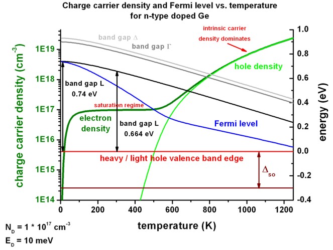
In this example, the effective density of states at 300 K was calculated as
follows:
Nc (300 K) = 61.068 * 1018 cm-3
Nv (300 K) = 5.411 * 1018 cm-3
This figure shows the same results as above, but this time the Fermi level is
set to a constant value EF = 0 eV.
Consequently, the conduction and valence band edges are plotted with respect to
the constant Fermi level.
This figure shows more clearly how the band edges align with respect to the
Fermi level.
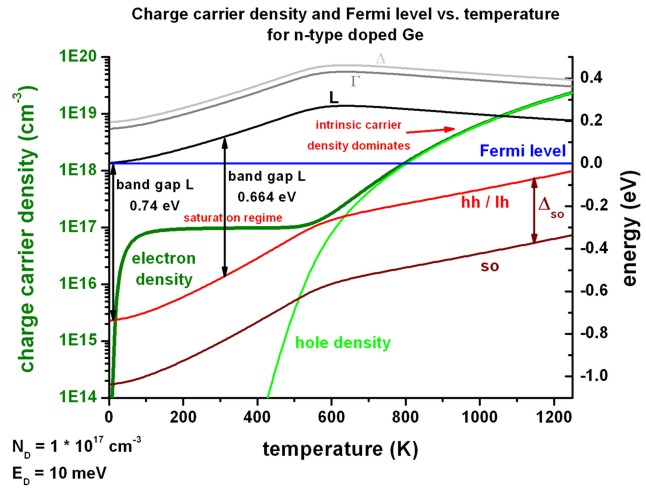
The data that has been plotted in the above shown figures can be found in
this file: sweep_temperature1D.dat
3b) Electron and hole concentration in doped Ge as a function of inverse
temperature 1/T
==> 1Dn_doped_bulk_Ge_b.in
   flow-scheme =
  14
: vary temperature as 1000/T
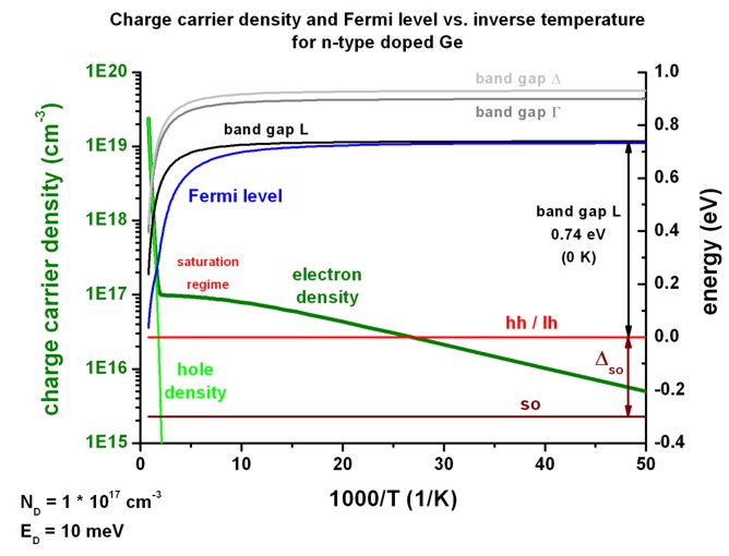
The same data as above is plotted but this time as a function of inverse
temperature in units of 1000/T.
The slope of the electron density approaches at high temperatures (i.e. left
side of the figure) the value of Egap/2 (if it holds Nc =
Nv which is not the case in our example).
At 300 K, Egap/2 = 0.332 eV.
At 600 K, Egap/2 = 0.267 eV.
At 900 K, Egap/2 = 0.200 eV.
At low temperatures the slope is ED/2 = 5 meV = 0.0005 eV.
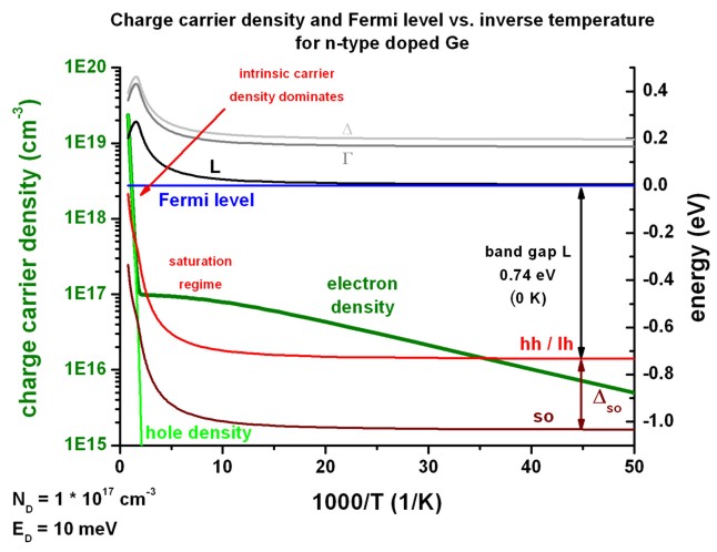
This figure shows the same results as above, but this time the Fermi level is
set to a constant value EF = 0 eV.
Consequently, the conduction and valence band edges are plotted with respect to
the constant Fermi level.
This figure shows more clearly how the band edges align with respect to the
Fermi level.
4) Compensated semiconductors - one donor level and one acceptor level
==> 1Dn_doped_bulk_Ge_a_compensated.in
   flow-scheme =
  13
: vary temperature as T
- An interesting situation occurs in real semiconductors that have both,
n-type and p-type doping. It is rather impossible to fabricate devices that
are merely n- or p-type because unintentional doping through impurities is
always present.
- We assume the same Ge sample as above, i.e. the Ge sample is n-type doped with a concentration of ND = 1 * 1017 cm-3.
The ionization energy of the donor ED is set to 10 meV.
In contrast to the above shown figures, also acceptors are present with
varying acceptor concentration ranging from
- NA = 1 * 1014 cm-3
(NA << ND) ==> ND
- NA =~ ND
- NA = 1 * 1016 cm-3
(NA < ND)
==> ND
- NA = 9*1016 cm-3
- NA = 5 * 1016 cm-3
(NA < ND)
==> ND
- NA = 5*1016 cm-3
- NA = 7 * 1016 cm-3
(NA < ND)
==> ND
- NA = 3*1016 cm-3
- NA = 9 * 1016 cm-3
(NA < ND)
==> ND
- NA = 1*1016 cm-3
- NA = 1 * 1017 cm-3
(NA = ND) ==>
ND - NA = 0
==> intrinisc density is recovered
The ionization energy of the acceptor EA is set to 10 meV.
- The following figure shows the electron density vs. temperature for
different acceptor concentrations NA.
Note that the donor concentration ND is kept constant.
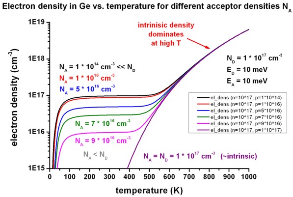
If NA = ND, then the intrinsic behavior of the
electron density is recovered. In any case, the intrinsic density dominates
at high temperatures.
In the saturation regime (between 100 K
and 400 K), the nominally dopant density (ND - NA)
determines the electron density.
The variation of the acceptor concentration is specified here:
	$doping-function

   doping-function-number = 2

   impurity-number        =
	2
	!
p-type impurity
   doping-concentration   = 0.0001d0
	! ND >> NA ! 0.0001 * 1018 / cm3
	= 1 * 1014 / cm3

 ! doping-concentration   = 0.01d0
	! ND >  NA ! 0.01   * 1018 /
	cm3 = 1 * 1016 / cm3

 ! doping-concentration   = 0.05d0
	! ND >  NA ! 0.05   * 1018 /
	cm3 = 5 * 1016 / cm3

 ! doping-concentration   = 0.07d0
	! ND >  NA ! 0.07   * 1018 /
	cm3 = 7 * 1016 / cm3

 ! doping-concentration   = 0.09d0
	! ND >  NA ! 0.09   * 1018 /
	cm3 = 9 * 1016 / cm3

 ! doping-concentration   = 0.1d0
	! ND =  NA ! 0.1    * 1018
	/ cm3 = 1 * 1017 / cm3
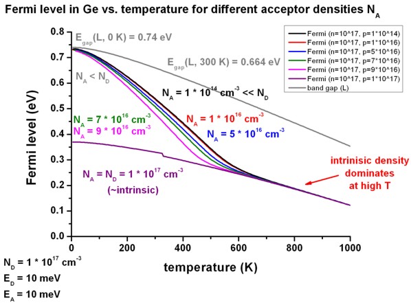
- The following figure shows the Fermi level as a function of temperature
for various acceptor densities NA.
Note that the indirect band gap at the L point decreases with temperature.
As expected, for the "intrinisic case" (ND
- NA = 0 ==> intrinisc
density is recovered), the Fermi level at 0 Kelvin lies in the
middle of the band gap at EF = 0.74 eV / 2 = 0.37 eV.
5) Compensated semiconductors - two donor levels and one acceptor level
==> 1Dn_doped_bulk_Ge_a_compensated_two_donors.in
   flow-scheme =
  13
: vary temperature as T
We assume a Ge sample which has two donor levels and one
acceptor level.
The acceptor concentration is NA = 4 * 1016 cm-3.
The ionization energy of the acceptor EA is set to 10 meV.
The donor concentrations ND,1 and ND,2 are varied.
The ionization energy of the upper donor level ED,1 is set to 10 meV.
The ionization energy of the lower donor level ED,2 is set to 100 meV.
We distinguish between three cases:
- 5a)
ND,1 = ND,2 = 5 * 1016 cm-3
> NA
=> ND,1 + ND,2 >
NA
- 5b)
ND,1 = 3 * 1016 cm-3
< NA
ND,2 = 7 * 1016 cm-3
> NA
ND,1 + ND,2
> NA
- 5c) (one donor level and one acceptor level)
ND,1 = 10 * 1016 cm-3
> NA
ND,2 = 0
- The following figure shows the result for these three cases. 5c) is
similar to the figures that have been discussed already.
At the dopant density of ND,1 - NA = 6 *
1016 cm-3 the saturation regime forms.
For case 5b) only the ionization of the second donor
level ED,2 is relevant at low temperatures.
For case 5a) two plateaus form:
- for the ionization of the upper donor level ED,1:
ND,1
- NA = 1 * 1016 cm-3
- for the ionization of the lower donor level ED,2:
ND,1 + ND,2 - NA = 6 * 1016
cm-3
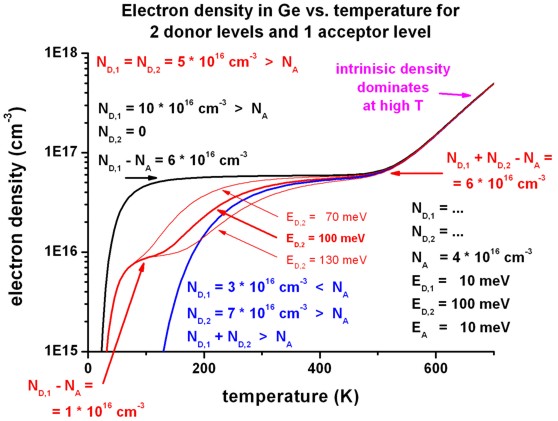
For comparison, for case 5a) the energetic position of the second donor
level ED,2 has been varied between 70 meV,
100 meV and 130 meV.
The energetic position of the upper donor level is at 10 meV.
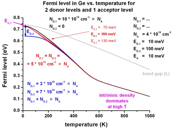
- The following figure shows the Fermi level for the cases 5a), 5b) and
5c).
The valence band edge is fixed at 0 eV. The indirect band gap at the L point
decreases with increasing temperature.
For case 5b), where only the ionization of the second
donor level ED,2 is relevant at low temperatures, one can
clearly see the position of the Fermi level at 100 meV below the conduction
band edge: EF (T = 0 K) = EC - ED,2
For case 5a) the Fermi level moves from the
upper donor level ED,1 at low temperatures to the lower donor
level ED,2 at around 200 K and start to ionize the second donor
level, eventually forming the second "plateau" in the electron density (see
figure above for the electron density).
At high temperatures, the Fermi levels moves approximately into the
middle of the band gap.
|