| nextnano.com nextnano³ Download | Search | Copyright | Publications * password protected |
nextnano³ software
|
|
| FAQ |
|
|
|
|
|
nextnano3 - FAQFrequently asked questionsGeneral
Materials
Simulation
GeneralProgram window closes immediately upon finishingQuestion Unfortunately, the program window that opens after I started Answer Yes, there is. In Windows go to the doesn't work at allQuestion I get a strange message in my command prompt. Something with "keyword", "optional", "required". Answer You are probably trying to run a UNIX formatted ASCII file on a PC (or vice versa). Save it in PC/DOS mode or download the PC formatted input files from the download section. Downloads / Additional toolsQuestion Where can I get the Perl script to convert output AVS/Express files (*.fld, *.dat, *.coord) into xyz files? Answer Follow this link to our download page: Downloads / Additional tools
| |||||||||||||||||||||||||||||||||||||||||||||||||||||||||||||||||||||||||||||||||||||||||||||||||||||||||||||||||||||||||||||||||||||||||||||||||||||||||||||||||||||||
| units | Reference | GaAs | AlAs | InAs | GaP | AlP | InP | GaSb | AlSb | InSb | GaN(zb) | AlN(zb) | InN(zb) | Si | Ge | C | ||
| EVBM | (eV) | Wei/Zunger | 1.46 | 0.95 | 1.52 | 0.99 | 0.45 | 1.10 | 2.03 | 1.61 | 2.02 | -0.72 | -1.52 | -0.46 | ||||
| DeltaSO | (eV) | Vurgaftman | 0.341 | 0.28 | 0.39 | 0.08 | 0.07 | 0.108 | 0.76 | 0.676 | 0.81 | 0.017 | 0.019 | 0.005 | 0.044 | 0.289 | ||
| Ev,av | (eV) | 1.346 | 0.857 | 1.390 | 0.963 | 0.427 | 1.064 | 1.777 | 1.385 | 1.750 | -0.726 | -1.526 | -0.462 |
If use-band-gaps = no (default), the conduction band energies for the Gamma, L and X valley are calculated as
conduction-band-energies = Egap(Gamma) + Ev,av+ 1/3 DeltaSO
Egap(X) + Ev,av + 1/3 DeltaSO
Egap(L) + Ev,av + 1/3 DeltaSO
|
|
The conduction band energies are given for 0 Kelvin in the nextnano³
database.
Varshni parameters should be used to get the temperature dependent
conduction band energies for e.g. 300 K.
With the specifier band-shift [eV], you are able to shift the
absolute values of valence and conduction band edges simultaneously by a certain amount (default: 0.0
eV).
For zinc blende, the three hole energies Ehh, Elh and Eso
(heavy, light and spin-orbit split-off energy) are related as follows:
(Ehh + Elh + Eso)/3 = Ev,av
For wurtzite, the three hole energies EA, EB and EC
(heavy, light and crystal-field split-off energy) are related as follows:
(EA + EB + EC)/3 = 2/3 * Deltacr + Ev,av
VBO: You can adjust valence-band-energies and/or
band-shift to adjust the valence band offset.
CBO: Option a) You can adjust conduction-band-energies (if
use-band-gaps = no) and/or band-shift
to adjust the conduction band offset.
Option b) You can adjust
band-gaps (if use-band-gaps = yes)
and/or band-shift and/or valence-band-energies adjust
the conduction band offset.
The situation for
ternaries is essentially the same.
Bowing parameters can be used to tune the band gaps and band offsets.
Additionally, a band-shift can be used.
(bow-conduction-band-energies, bow-valence-band-energies,
bow-band-shift, band-shift)
For ternaries, the Varshni parameters are not interpolated. Instead, the
conduction-band-energies (if use-band-gaps =
no) are interpolated (default) or the band-gaps (if
use-band-gaps = yes).
In order to get the valence band edges for ternaries, the following procedure applies.
[eV] - average valence band edge energy Ev,av: valence-band-energies
= ... [eV]
- split-off energy Deltaso: 6x6kp-parameters =
. . . DeltaSO
[eV]
- absolute deformation potential:
absolute-deformation-potential-vb = ... [eV]
- uniaxial deformation potentials: uniax-vb-deformation-potentials
= ... [eV]
- band-shift: band-shift = ...
[eV] (Typically, the default value is zero.)How is nonparabolicity treated?
The following parameters of the database refer to a hyperbolic dispersion, k2 ~ E(1+aE) where
a = nonparabolicity [1/eV].
conduction-band-nonparabolicities = 0d0 0d0 0d0 !
valence-band-nonparabolicities = 0d0 0d0 0d0 !
They are only used in regions where the density is calculated classically.
The do not enter the Schrödinger equation.
In order to treat nonparabolicty in quantum regions, a 6-band k.p or
8-band k.p model is required.
A common problem is that for the smaller band gap
semiconductors like InAs, the nonparabolicity is so large that the calculated Fermi levels
(to be precise: the calculated alignment of the band edges with respect to the
Fermi level) are quite inaccurate.
For example, when looking at a case with n~1.5x1018 cm-3,
the Fermi level calculated without nonparabolicity is about 0.214 eV. It is 0.143 eV
when nonparabolicty is taken into account.
Here is an example of how one can modify the Fermi-Dirac integral for free
carrier concentration in 3D for a single band from parabolic to nonparabolic
using the Van Halen-Pulfrey functions. The nonparabolicity modifies the SQRT(E)
density of states in the simple way shown.
How are effective hole masses determined in the database? By k.p
parameters (6x6/8x8kp-parameters) or by effective masses (valence-band-masses)?
In the database when we describe material we specify
But they are not consistent: k.p parameters are used only when 6-band
or 8-band
k.p quantum model is selected and hole effective masses are used only
when 1-band Schrödinger equation is solved.
(Exception: The k.p parameter Deltaso for spin-orbit
splitting energy is used in any case including if no strain is considered.
The k.p parameters in the database are also used to determine band shifts
due to strain. Program computes the k.p and strain dependent Hamiltonian
for each grid point, diagonalizes it, and takes the eigenvalues for the band
edges. So, band edges for single band calculations are k.p parameter
dependent. More
information ...)
There is also the option under
$numeric-control
to calculate the effective valence band masses from the 6-band k.p
parameters (L, M, N) specified in the
database.
Question
For the quantum calculation there is a possibility to choose either Dirichlet
or Neumann boundary conditions. Which function is a subject for such boundary
conditions? Wave function? If yes, do Dirichlet
conditions mean that wave
function is equal to zero on the boundaries?
Answer
Yes, at the boundaries of the quantum region, the wave function is zero if Dirichlet
is chosen.
Neumann:
- Physically, it means zero current normal to the boundary surface (3D),
boundary line (2D) or boundary point (1D).
- Mathematically, it means if a Hamiltonian contains a term like
[d/dxi mij d/dxj +
bi d/dxi + c] Psi
then the boundary condition is
[ni mij d/dxj + bi
ni] Psi = 0
where ni is a normal vector to a
surface (line).
More details about boundary conditions can be found here:
Boundary
conditions
Question 1
In 1D, what is the unit of doping concentration? If I have an experimental value of 2*1018 cm-3 for 3D, is it then 21/3*106 cm-1 for 1D?
Answer 1
No, it is still 2*1018 cm-3 for 1D. Please look at this
example for more details:
$doping-function
Error message Error linesearch: Round-off problem.
Solution
This error occurs in the Newton routine (subroutine linesearch) when solving the 1D/2D/3D nonlinear Poisson equation with the Newton method.
Possible solutions (depending on your input file geometry):
$numeric-control
...
nonlinear-poisson-stepmax = 1.0d-0
nonlinear-poisson-iterations = 100
$end_numeric-control
phiV under the keyword
$numeric-control
(specifier initial-potential).
Error message (on Windows only)
forrtl: error (74): floating underflow
forrtl: error (74): floating underflow
forrtl: info (300): 9 floating underflow traps
Explanation
An underflow indicates that the absolute value of a floating point number has become smaller than about 1e-150 and that it has been replaced by a zero. For many algorithms this replacement does not cause any harm, for others the effects will be disastrous. Unfortunately, in simulation codes like nextnano3 both cases occur depending on where in the code the underflow happened.
Question
I want to manually adjust the Fermi level. How can I do this?
Answer
There are several possibilites.
$import-data-on-material-grid$region-cluster
$quantum-clusterFermi)
or a linear Fermi level profile (Fermi-linear).
$poisson-boundary-conditionsThese four options can also be combined.
An example is shown here: Double quantum well heterostructure
1DAlGaAs_GaAs_DQW_read_in_Fermi_level.in
1DAlGaAs_GaAs_DQW_apply_Fermi_level_to_region_cluster.in
1DAlGaAs_GaAs_DQW_apply_Fermi_level_to_quantum_cluster.in
1DAlGaAs_GaAs_DQW_apply_Fermi_level_to_contact.in
If you are interested in examples, please submit a support ticket.
Question
I have to simulate a quantum dot with [N 1 1] growth direction.
But in the database I have only:
axes-possible = 0 0 1 !
0 1 0 !
1 0 0 !
Is it possible to simulate [N 1 1] growth direction?
Answer
Yes, but don't confuse the axes-possible specifier with the
Miller indices. Change these to [N 1 1] for other directions.
The specifier axes-possible is only applicable to the growth
direction which must be x, y or z as indicated. However, you can choose [3
1 1] to be the Miller x axis and then choose x axis as growth direction
which will then be [3 1 1].
More details can be found under keyword
$domain-coordinates.
Question
What should I pay attention to?
Answer
GaAs-4K in
addition to GaAs in the database). bow-conduction-band-energies = 0.305d0 0.055d0
0d0
The bowing factor for the Gamma band (according to
Vurgaftman is)0.384d0 for Al0.39Ga0.61As
-> Crossover for minimum (Gamma -> L) at x=0.39
(300 K) 0.305d0 for Al0.33Ga0.67As
-> (Gamma) 0.070d0 for Al0.15Ga0.85As
-> (Gamma)Question
Can I use Matlab to visualize the 3D output files (AVS format)?
Answer
Not directly, but you should be able to convert the AVS data to Matlab format if you write a script that does it for you. For an explanation of the AVS format, please consult the 2D/3D Tutorials.
Question
I want to "switch-off" piezoelectrical effects. Should I put
piezo-electric-constant e14 in the database_nn3.in
file to be 0, or can I specify it somewhere in the input file?
Answer
Option 1: You have to adjust e14 for the appropriate materials in the
database_nn3.in file to:
piezo-electric-constants = 0d0 0d0 0d0
0d0 ! [C/m²] e14,B114,B124,B156
Option 2: You can specify it here:
$numeric-control
piezo-constants-zero = no
The pyroelectric constants can be switched on and off similarly.
Question
Are quaternaries included? If not, how can I interpolate them?
Answer
Only lattice matched-quaternaries (e.g. InxGayAl1-x-yAs with only one free parameter x or y but not quaternaries with two free parameters like AxB1-xCyD1-y) are included in our database. See database comments and quaternaries documentation.
You can define a new material in the
database_nn3.in file with linearly interpolated values of the binary
constituents of the quaternary.
Question
How do you incorporate strain into the calculation? What is the meaning of the deformation potentials in the database?
Answer
In order to get the band edge shifts due to strain, we diagonalize numerically on each grid point the strain dependent k.p Hamiltonian for k=0. More information ...
Van de Walle (PRB 39, 1871 (1989)) describes the dependence on strain of the valence and conduction band edges (zinc blende). In this paper strain is described along [001] and [111] directions. In a general case, when we have [a b c] growth direction please have a look here.
Pseudomorphic (or commensurate) growth of strained layers on a substrate subjects these layers to a biaxial strain (epsilon||) parallel to the plane of the interface and a uniaxial strain (epsilon|_) perpendicular to it.
![]() (1)
(1)
where a||=a0 (2a)
![]() . (2b)
. (2b)
So we can also write
![]()
![]()
Here a0 denotes the lattice constant of the substrate and a the equilibrium lattice constant of the layer material. D depends on the elastic constants c of the layer material and on the interface orientation. (Often, 1/D001 is called the Poisson ratio, denoted as sigma).
![]() (3a)
(3a)
![]() (3b)
(3b)
![]() (3c)
(3c)
In the database we specify:
| for zinc blende | for wurtzite | units | |
lattice-constants |
a a a | a a c | nm |
elastic-constants |
c11 c12 c44 | c11 c12 c13 c33 c44 | GPa |
The lattice constants are temperature dependent. More information...
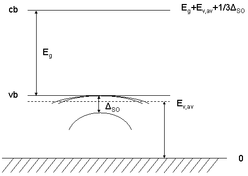
The effect of strain on energy levels can be decomposed into hydrostatic and shear contributions. The hydrostatic strain component leads to a shift of the average valence band energy Ev,av=(Ehh+Elh+Eso)/3, i.e. of the average of the energies of the heavy hole, light hole and spin-orbit split-off bands (see picture for details):
![]() (4a)
(4a)
and similarly for the conduction band energy
![]() (4b),
(4b),
where av and ac are the hydrostatic (=absolute) deformation potentials for the valence band and conduction band, respectively.
In the database we specify:
| valence bands | conduction bands | |||
| Gamma | L | X | ||
absolute-deformation-potential-vb |
av | |||
absolute-deformation-potentials-cbs |
ac(Gamma) | ac(L) | ac(X) | |
The shear contribution couples to the spin-orbit interaction and leads to an additional splitting of the valence band energies. In the case of growth on a (001) or (111) substrate, the energy shifts relative to Ehh=Ev,av+Deltaso/3 (Deltaso is the spin-orbit splitting in the absence of strain) are given by
![]() (5a)
(5a)
![]() (5b)
(5b)
![]() (5c)
(5c)
The strain dependent shift delta Esh depends on the interface orientation:
![]() (6a) or
(6a) or
![]()
![]() (6b) or
(6b) or
![]()
Here,
![]() .
.
The quantities b and d are the tetragonal and rhombohedral shear deformation potentials, respectively. In the absence of strain, equation (5) leads to the correct spin-orbit splitting Deltaso. Conduction bands at Gamma are not affected by the shear contribution to the strain. However, at L and X they are affected.
In the database we specify:
| valence bands | conduction bands | |||
| Gamma | L | X | ||
uniax-vb-deformation-potentials |
b d | |||
uniax-cb-deformation-potentials |
0 (always zero) | Xiu(L) | Xiu(X) | |
valence-band-energies |
Ev,av (eV) | |||
conduction-band-energies |
Ev,av+ 1/3 DeltaSO+ Egap(Gamma) |
Ev,av+ 1/3 DeltaSO+ Egap(L) |
Ev,av+ 1/3 DeltaSO+ Egap(X) |
|
6x6kp-parameters |
..... .....
..... Deltaso (eV) |
|||
8x8kp-parameters |
..... ..... ..... ..... .... ..... |
|||
Once Ev,av are known on an absolute scale (only physically meaningful relative to Ev,av in related semiconductors), the valence band and conduction band edge energies Ev and Ec, respectively, are obtained on an absolute scale from
![]() (7a)
(7a)
![]() (7b) (for Gamma)
(7b) (for Gamma)
where Ev,av, Deltaso, and Eg
(band gap energy) refer to unstrained bulk properties. The strain contribution
is incorporated into the other properties.
Now we can calculate the band offset at the interface directly comparing the
values of Ev and and Ec of the
semiconductors constituting the heterojunction.
Equations (4), (5) and (6) were arrived at by treating the effect of strain as a small perturbation, and are therefore only valid in the case of small lattice mismatch. The mismatch attainable in pseudomorphic heterojunctions composed of III-V alloys is expected to fall within this range of validity.
(Most of this text was taken from M.P.C.M. Krijn, Semicond. Sci. Technol. 6, 27 (1991))
Question
Is it possible to have some of the layers of the heterostructure to be
pseudomorphic and then at some point higher up in the structure have the layers
be relaxed? Currently, I have the entire structure with
homogeneous-strain.
Answer
Yes, it is. Have a look at this keyword:
$material
For each material one can specify its own substrate. If this substrate is
identical to the material name, then one has a "relaxed" and not a strained
material, even with option homogeneous-strain.
Question
How can I specify the substrate or its lattice constant?
Answer
$domain-coordinates<material-name>
...
pseudomorphic-on =
...
$end_domain-coordinates
Question
I want to simulate a superlattice of quantum wells in 1D. For this I want to build a cluster consisting of a well and a barrier, i.e. this cluster would contain 2 different materials. Is this possible?
Answer
No. You can define one huge cluster that consists of the barrier
material for the whole superlattice and set region-priority=1. Then
you can put several wells on it with region-priority=2.
Alternatively, open two windows of the
1D Input
file generator (Step 1) and define in the first the barrier and in the
second the well and press the "Submit" buttons alternately.
Question
What physical properties or equations are affected if I change the
lattice-temperature
in the input file?
Answer
varshni-parameters-on = no.
database_nn3.in file to get the correct band gap for the corresponding
temperature of interest (more information on
band gap). You can even specify your own materials as was already done for
GaAs-4K, AlAs-4K, InAs-4K, Al(x)Ga(1-x)As-4K, In(x)Ga(1-x)As-4K,
Al(x)In(1-x)As-4K (in addition to GaAs, AlAs, ...).
$impurity-parameters specifies how far a donor/acceptor lies
below/above the conduction/valence band. If the temperature is around 4 K,
almost no donors/acceptors are ionized. In this case - if you still want all
donors/acceptors to be fully ionized - you need to specify a value of say -10
eV instead of +0.03 eV.
$numeric-control
(lattice-constants-temp-coeff-on = no/yes).
Question
When we have 2D simulation we can specify as simulation domain [1 0 1]
or [1 1 0 ] or [0 1 1]. What is x
and what is y in the simulation domain?
Answer
| [x y z] | simulation system | calculation sytem = x,y system |
| [1 0 1] | (x,z)-plane | x=x, y=z |
| [1 1 0] | (x,y)-plane | x=x, y=y |
| [0 1 1] | (y,z)-plane | x=y, y=z |
Question 1
How to plot 2D AVS/Express output data with Origin? ->
Answer
Question 1
What is the unit of the electron density (output)? What is the units of the elastic constants in the database?
Answer 1
The electron/hole density output will be given in the following units
[1018
cm-3].
These units are the same for 1D, 2D and 3D simulations.
The elastic constants are given in GPa.
Question 2
The numbers of the electron density on my plot looks different to what I expected.
Answer 2
You could try to adjust your energy-levels-relative in
impurity-parameters
to -10d0 instead of e.g. 0.02d0 and
check if it makes a difference.
Question 3
I get three different columns for my electron density output (1D) when I run a quantum mechanical calculation. Which one is the electron density?
Answer 3
The second column in the electron density which is the sum of
classical and quantum mechanical density.
- second column: sum of quantum mechanical and classical density
- third column: quantum mechanical density
- forth column: classical density
Warning define_poisson_clusters: Boundary conditions fixed manually, not
by input.Question
I get the following warning:
Warning define_poisson_clusters: Boundary conditions fixed manually, not
by input.What does it mean?
Answer
It simply means that for the boundary conditions of the Poisson equation ($poisson-boundary-conditions)
by default Neumann boundary conditions with electric field = 0 V/m
are assumed when calling SUBROUTINE define_poisson_clusters. This
is just a reminder that these boundary conditions cannot be specified in
the input file yet. However, Ohmic and
Schottky boundary conditions are implemeted correctly.
Question
Why does it take so long to calculate the eigenvalues of an 8-band k.p calculation?
Answer
Mathematically speaking, 8-band k.p requires a different eigenvalue solver (“finding eigenvalues in the interior of the spectrum”) than single-band and 6-band (“finding eigenvalues at the end of the spectrum”), so it is much harder (both with respect to time and stability) to find a solution.
An 8-band matrix has 8 times the size of a single-band matrix and the mathematical problem gets harder the more eigenvalues are sought.
We have implemented different eigenvalue solvers for 8-band k.p, e.g. the ARPACK solver (shift-invert mode) or the FEAST solver.
Degeneracy: For instance, if 4 eigenvalues are degenerate (e.g. due to spin and/or geometry) and you are looking for only 3, the eigenvalue solver will very likely fail. In such a case, it could be that certain eigenvalues are misisng.
Adjusting the resdiual might help you for debugging, e.g. by using a larger value for the residual (accuracy) one should get solutions more quickly althouth they might not be accurate enough.
Another interesting strategy could be to divide the input file into two, e.g.
if one needs 6 electron eigenvalues and 12 hole eigenvalues.
- One input file calculates only the electron eigenvalues. Then you have in total 6 eigenvalues instead of 18 which should be much faster.
- The other input file calculates only the hole eigenvalues. (12 instead of 18)
|
|